|
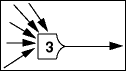
Figure 5. Threshold gate.
The most direct way to see how discrete threshold
gates combine to make an effective logic circuit
is via an example. The half adder will serve as
the example and relate the single data value form
of NULL Convention Logic to traditional Boolean
logic. Figure 6 shows a conventional Boolean logic
half-adder circuit with its clock, and Figure
7 shows a NULL Convention Logic half-adder circuit.
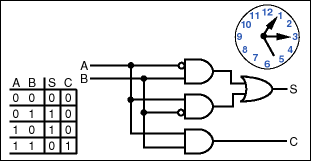
Figure 6. Boolean logic half-adder circuit
with clock.
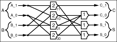
Figure 7. NULL Convention half-adder circuit.
The Boolean half-adder circuit expresses four
possible input data values with two data values
(0, 1) on two wires (A, B). The
NULL Convention half-adder circuit expresses the
same four possible input data values with
one data value (DATA) on four wires (A_0,
A_1, B_0, B_1). Each binary data value A,
B, C and S is expressed by a mutually exclusive
assertion group of two wires (A_0, A_1 and
B_0, B_1 and C_0, C_1 and S_0, S_1). Only
one wire in each group can assert DATA at a time,
so a complete input data set for the circuit is
two DATA values, one from each group (A and
B). The completeness of input criteria for
each threshold 2 gate is two DATA values. It can
be seen that for any threshold 2 gate to assert
a data result value there must be one DATA value
asserted in each input group and that only one
threshold 2 gate at a time will assert a result
data value as long as the mutually exclusive assertion
convention is enforced for the input groups. The
gates, as well as the circuit as a whole, enforce
the completeness of input criteria for data. When
the result values transition from NULL to a complete
result data set, which in this case is
one DATA value for each result group (C and
S), then the asserted result values are a
correct resolution of a complete input data set.
The completeness of input criteria for each gate
scales up for the circuit as a whole and as before,
the completeness of resolution can be determined
by simply monitoring the result values. Figure
8 shows the circuit behavior for all four possible
input combinations. Bold lines are asserting DATA
and thin lines are asserting NULL. |