Again,
the behavior of each gate scales up for the circuit
as a whole. Refer to Figure 2 again and assume
each gate is an Intermediate value gate. Beginning
with the circuit in an all data state, if only
D becomes NULL gate 1 will assert an intermediate
value until C also becomes NULL. If a single input
value remains data there will be at least one
result value that remains Intermediate. When all
result values become NULL it means that the input
values are all NULL and the NULL values have propagated
through the circuit and that the circuit is in
a completely NULL state. The circuit as a whole
enforces the completeness of input criteria for
both data in relation to NULL and for NULL
in relation to data.
It can now be determined when the circuit is completely
reset to NULL and ready to accept a new input
data set to resolve by simply monitoring the result
values. When the result values transition from
a complete result data set to all NULL the circuit
is completely reset and ready to accept a new
data set. The circuit indicates its own readiness
to accept a new input data set purely symbolically
and autonomously. No expression or authority
external to the circuit expression such as a clock,
delay line or controller is needed.
We now have a circuit that is a complete expression
in and of itself. It can tell the world when it
is ready to accept data to resolve, and it can
tell the world when it has completed a data resolution.
Data resolution occurs in an orderly wave front
of correct result values within the circuit. It
can be a fully autonomous and asynchronous element
of a larger whole (i.e., a system).
An intermediate value logic circuit is a symbolically
complete process expression and is purely symbolically
determined. The Intermediate value solution is
a theoretically complete and general solution
to delay insensitive circuit synthesis. Its symbol
resolution behavior is not affected in any way
by the propagation delay of any element in an
expression.
The addition of the NULL value or the Intermediate
value did not change the transform specifications
for the data values. Intermediate value NULL Convention
Logic gates can replace the gates of a standard
Boolean logic combinational circuit one for one,
and the circuit will provide the identical logic
function as before. It will simply resolve in
a more orderly manner and assert its own completion,
as well as its own readiness to accept a new input
data set.
The Feedback Solution
The feedback solution makes each gate a state
machine with hysteresis of result value assertion.
Figure 4 shows the truth table for the feedback
gate. Do not be daunted by the seeming complexity
of this table. This is just the first example
to introduce the NULL convention.
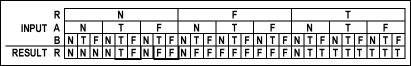
Figure
4. The feedback gate and its truth table.
R is the result variable fed back to the input.
When the gate is asserting NULL it is in the NULL
(N) state and will continue asserting
N until both input values become data (T,F)
at which point it will transition its result value
to a data value and enter a data state. When the
gate is in a data state (R=F or T)
it will continue asserting a data value until
both input values become NULL (N)
at which point it will transition its result value
to N and enters a NULL state. The feedback
gate enforces the completeness of input criteria
for both data in relation to NULL and
for NULL in relation to data.
Again, the behavior of each gate scales up for
the circuit as a whole. Refer to Figure 2 again
and assume each gate has feedback. Beginning with
the circuit in an all data state, if only D becomes
NULL gate 1 continues to assert a data value until
C also becomes NULL. If a single input value remains
data there will be at least one result value that
remains data. When all result values become NULL
it means that the input values are all NULL and
the NULL values have propagated through the circuit
and that the circuit is in a completely NULL state.
The circuit as a whole enforces the completeness
of input criteria for both data in relation to
NULL and for NULL in relation to data.
A Non-Critical Time Relationship
While the intermediate value solution uses play
through gates with no time relationships at all
and is fully delay insensitive, the feedback solution
is not fully delay insensitive in that there is
a non-critical time relationship involved.
The feedback path around each gate must stabilize
faster than successive wave fronts of transition
pass through the circuit as a whole. We call this
a non critical time relationship because it is
easy to achieve since the circuit propagation
time will typically be much longer than the feedback
propagation time. The feedback solution is not
purely delay insensitive but is effectively delay
insensitive. |