The
Data Resolution Wavefront
The completeness of input criteria is the key
to speed independent logic circuits. The completeness
of input criteria for each gate scales up for
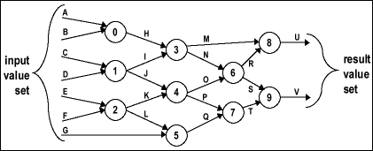
combinational circuits as a whole. Consider Figure
2.

Figure 2. Example of a combinational circuit.
Assume that the circuit is in an all NULL state
in that all of the input values, internal values
and result values are all NULL. If one input value,
A for instance changes to data, gate 0 will continue
asserting a NULL value. Gate 0 does not assert
a data value until both input values for A and
B are data. To see how this behavior scales up
for the whole circuit consider gate 6. Gate 6
will not assert a data value until both inputs
N and O are data at the gate. It doesn't
matter how long it took for the data values on
N and O to propagate to the gate 6 input or in
which order they arrive. When both input values
are data at gate 6, it asserts the correct result
data value. This transition from NULL to data
also asserts the validity of that result data
value and asserts the completion of gate's resolution
entirely symbolically. No other aspect of expression
and no time relationship is associated with the
assertion of these three facts. Each gate is a
synchronization node managing an orderly
wave front of correct result values propagating
through the circuit.
The circuit as a whole will not assert a complete
set of result data values until there is a complete
set of input data values and the resolution of
the input data values has propagated through the
circuit. If one input value remains NULL at least
one result value will remain NULL. For instance,
if all the input values are data except G, which
remains NULL, then gate 5 will assert a NULL result
value for Q, gate 7 will assert a NULL result
value for T and gate 9 will assert a NULL result
value for V. When G becomes data, the input data
set is complete. The data value will propagate
through the circuit and V will become data and
the result data set will be complete (all
datas, no nulls).
When all the result values become data, it means
that a complete set of input data values are presented
to the circuit, that the resolution of the presented
input value set is complete and the asserted set
of result values is the correct and valid resolution
of the presented set of input data values. This
is what is meant by the completeness of input
behavior of each gate scaling up for a circuit
as a whole. The circuit does not assert a complete
set of result data values until a complete set
of input data values are present at the input
to the circuit and resolution of the input values
is complete. The circuit as a whole enforces
the completeness of input criteria for data.
The completion of resolution of an input data
set can be determined by simply monitoring the
result values. When the result values transition
from all NULL to a complete result data value
set (all data at the output), then the
resolution of a complete set of input data values
is finished. The circuit indicates its own
completion of resolution, autonomously and purely
symbolically. No external expression or authority
such as a clock, delay line or controller is needed. |